GPU Memory Hierarchy Part 1: Understanding the Foundations
Introduction to GPU memory hierarchy and the fastest memory types - registers, shared memory, and L2 cache
Modern deep learning depends heavily on GPUs, but understanding how GPUs manage memory is crucial for optimizing model performance. This three-part series explores the memory hierarchy in GPUs, focusing on the NVIDIA A100 architecture.
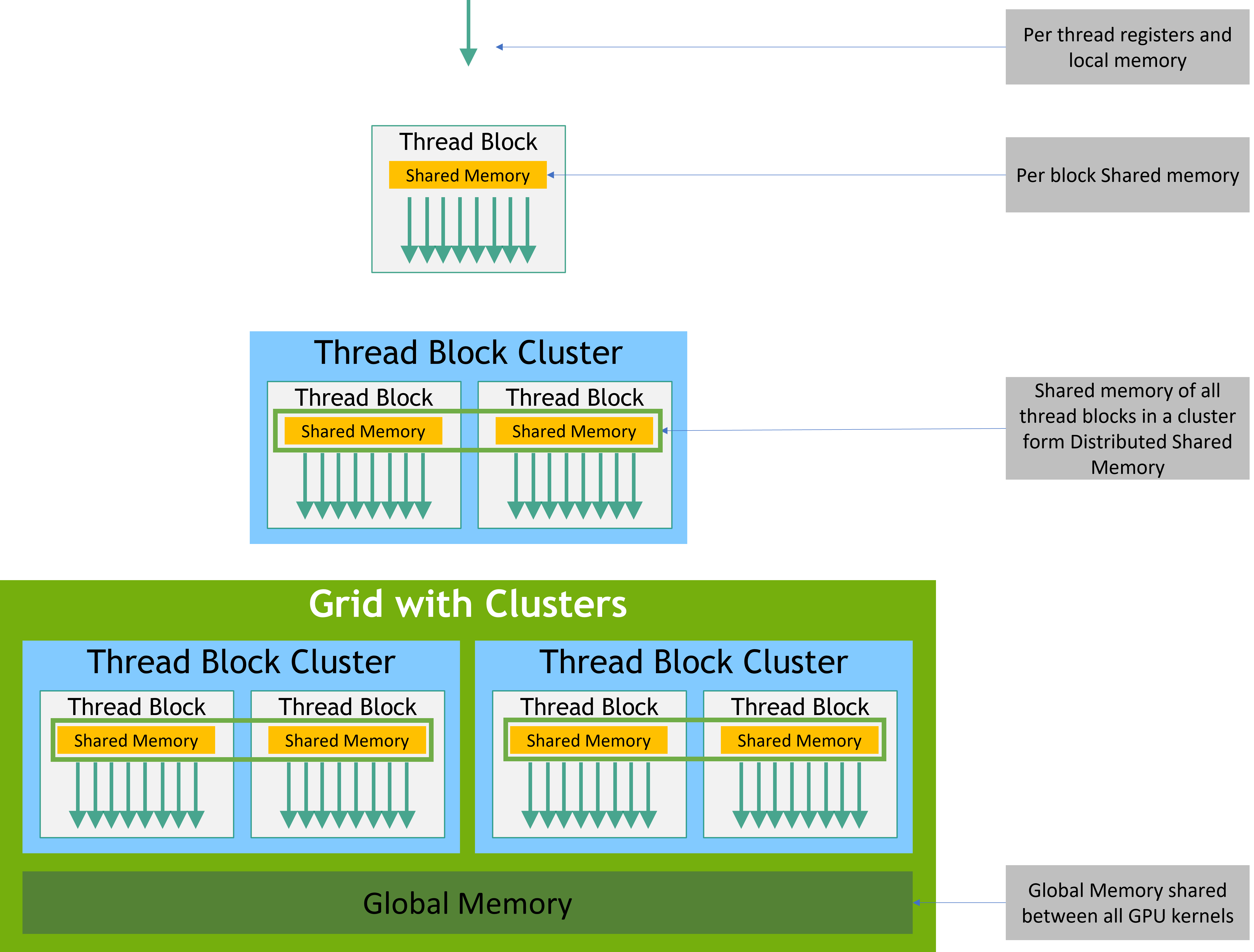
GPU Memory Hierarchy (Source: NVIDIA CUDA Programming Guide)
What is GPU Memory Hierarchy?
GPU memory hierarchy is a structured system of different memory types, each with distinct characteristics in terms of speed, capacity, and energy consumption. Think of it like a library system:
- Registers: Your desk (immediate access, tiny capacity)
- Shared Memory: Books on your desk (very fast, limited space)
- L2 Cache: Bookshelf in your room (fast, moderate space)
- Global Memory/HBM: Library shelves (large capacity, slower access)
Understanding this hierarchy is essential because memory access time often dominates computation time in deep learning workloads.
Why Memory Hierarchy Matters
The Performance Paradox: Modern GPUs can perform trillions of operations per second, but if data isn’t available when needed, those compute cores sit idle. This is the memory bottleneck problem.
Key Insight: A model that efficiently uses the memory hierarchy can run 10-100× faster than one that doesn’t, even with identical FLOPs (floating-point operations).
Real-World Impact:
- Training time: Hours vs days
- Inference latency: 10ms vs 100ms
- Energy consumption: Dollars vs cents per inference
- Deployment feasibility: Runs on device vs requires cloud
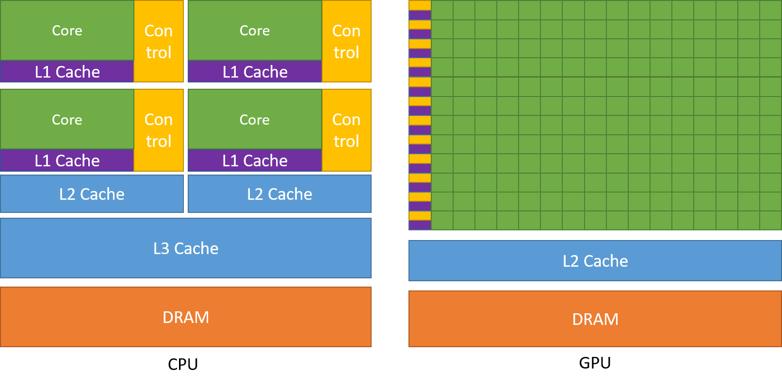
GPUs devote more transistors to computation vs control (Source: NVIDIA CUDA Programming Guide)
The Fast Layer: Registers
What are Registers? Registers are the smallest, fastest memory units directly accessible by GPU cores. Each thread has its own private set of registers.
Characteristics:
- Access Speed: Fastest - essentially instantaneous
- Access Time: 1-2 cycles
- Energy Consumption: Lowest - minimal power per access
- Capacity: Limited to several KB per thread block (~64KB per SM on A100)
- Scope: Private to individual threads
How Registers Work: Think of registers as the calculator buttons you’re currently pressing. Every intermediate calculation during a computation gets stored here temporarily.
Example in Transformers: During self-attention computation, when calculating the dot product between a query vector and key vector:
\[\text{score} = q_i \cdot k_j = \sum_{d=1}^{d_k} q_i^{(d)} \times k_j^{(d)}\]Each individual multiplication ($q_i^{(d)} \times k_j^{(d)}$) and the running sum are stored in registers.
Why This Matters: Keeping data in registers avoids expensive memory reads. Well-optimized CUDA kernels maximize register usage for frequently accessed values.
Limitations:
- Very limited capacity
- If a thread needs more registers than available, “register spilling” occurs (data moves to slower memory)
- Register pressure can limit parallelism
Shared Memory: Fast Collaboration
What is Shared Memory? Shared memory is on-chip memory shared by all threads within a thread block. It’s explicitly managed by programmers for optimal performance.
Characteristics:
- Access Speed: Very fast
- Access Time: 4-8 cycles
- Energy Consumption: Low
- Capacity: Up to 100 KB per SM (Streaming Multiprocessor)
- Scope: Shared within a thread block
How Shared Memory Works: Imagine a whiteboard in a team meeting room. All team members (threads in a block) can read and write to it, enabling fast data sharing without going to the main database (global memory).
Example in Transformers: During multi-head attention, the Query (Q), Key (K), and Value (V) matrices are loaded into shared memory:
1
2
3
4
5
6
7
8
9
# Conceptual CUDA-like pseudocode
__shared__ float shared_Q[BLOCK_SIZE][D_MODEL];
__shared__ float shared_K[BLOCK_SIZE][D_MODEL];

# Load Q and K into shared memory
shared_Q[threadIdx.x] = Q[blockIdx.x * BLOCK_SIZE + threadIdx.x];
shared_K[threadIdx.x] = K[blockIdx.x * BLOCK_SIZE + threadIdx.x];

# All threads in block can now access shared_Q and shared_K efficiently
Optimization Techniques:
- Tiling: Break large matrix multiplications into tiles that fit in shared memory
- Data reuse: Load data once, use many times
- Coalescing: Coordinate memory access patterns across threads
Why This Matters: Loading frequently reused data (like attention matrices) into shared memory once and reusing it multiple times dramatically reduces global memory accesses. This can provide 10-50× speedup for memory-intensive operations.
Limitations:
- Limited capacity (100 KB on A100)
- Requires explicit programming (not automatic)
- Bank conflicts can reduce performance if not careful
L2 Cache: The Smart Intermediary
What is L2 Cache? L2 cache is a larger, automatically managed cache shared across all Streaming Multiprocessors (SMs) on the GPU.
Characteristics:
- Access Speed: Moderate (faster than global memory, slower than shared memory)
- Access Time: 30-50 cycles
- Energy Consumption: Moderate
- Capacity: ~6 MB on A100 (shared across all SMs)
- Scope: Shared globally across the entire GPU
How L2 Cache Works: L2 cache automatically stores recently accessed global memory data. Think of it as a “recently used items” shelf in a warehouse - items you grabbed recently are kept nearby for faster re-access.
Example in Transformers: During the forward pass, if layer normalization parameters ($\gamma$ and $\beta$) are accessed multiple times:
\[\text{LayerNorm}(x) = \gamma \frac{x - \mu}{\sqrt{\sigma^2 + \epsilon}} + \beta\]The $\gamma$ and $\beta$ parameters, once loaded from global memory, are cached in L2 for subsequent accesses.
Cache Hit vs Cache Miss:
- Cache Hit: Data found in L2 → 30-50 cycles
- Cache Miss: Must fetch from HBM → 200-400 cycles
Why This Matters: L2 cache provides a significant speedup (4-8×) for frequently accessed data without requiring explicit programming (unlike shared memory). The GPU hardware automatically manages what gets cached.
Optimization Strategy: Structure your algorithms to maximize data reuse within a short time window to keep data “hot” in the L2 cache. Sequential access patterns and temporal locality are key.
Speed Comparison
To understand the performance gap between these memory types:
| Memory Type | Access Time | Relative Speed | Energy Cost |
|---|---|---|---|
| Registers | 1-2 cycles | 200× faster than Global | Lowest |
| Shared Memory | 4-8 cycles | 50× faster than Global | Very Low |
| L2 Cache | 30-50 cycles | 5-8× faster than Global | Low |
| Global Memory | 200-400 cycles | Baseline | High |
Key Insight: A single global memory access takes as long as 100-200 register operations. This massive speed difference is why memory optimization is crucial for GPU performance.
Real-World Performance Impact
Consider a matrix multiplication operation in a Transformer model:
Without Optimization (Naive Global Memory Access):
- Each element requires 2N global memory reads
- Time per element: ~400 cycles × 2N = 800N cycles
With Shared Memory Tiling:
- Load tiles into shared memory once
- Reuse data N times from shared memory
- Time per element: ~400 cycles (load) + 8 cycles × N (reuse) ≈ 400 + 8N cycles
Speedup: For N=64, speedup is (800×64)/(400+8×64) ≈ 56× faster!
Key Takeaways
Memory Hierarchy Fundamentals: GPU memory is organized in a speed-capacity trade-off hierarchy. Faster memory (registers, shared memory) has tiny capacity, while slower memory (global memory) has huge capacity.
Performance Impact: The 100-200× speed difference between registers and global memory means memory access patterns often matter more than computation speed.
Optimization Strategy: The key to GPU performance is keeping data in faster memory tiers as long as possible and minimizing trips to global memory.
Programming Models:
- Registers: Automatic (compiler managed)
- Shared Memory: Explicit (programmer controlled)
- L2 Cache: Automatic (hardware managed)
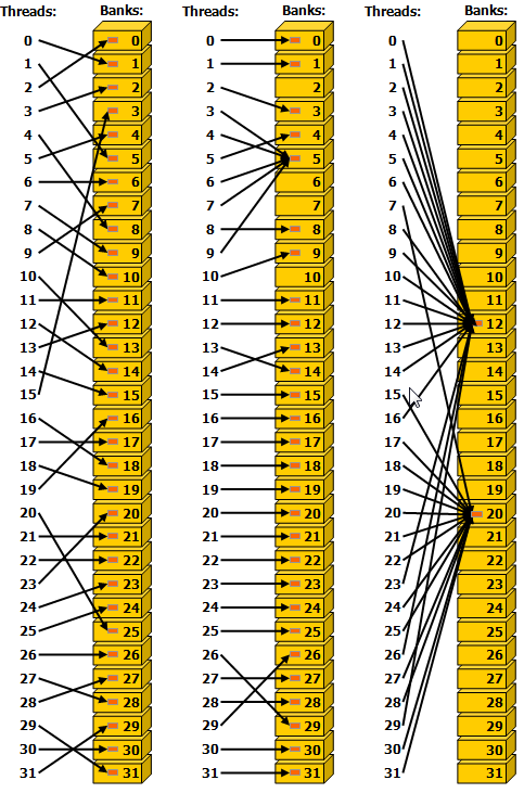
Shared memory access patterns (Source: NVIDIA CUDA Programming Guide)
What’s Next?
In Part 2, we’ll explore the larger, slower memory types: Global Memory, HBM, Texture Memory, and Unified Memory, along with comprehensive comparison tables.
Series Navigation:
- Part 1: Understanding the Hierarchy (Current)
- Part 2: Global and Specialized Memory
- Part 3: Optimization and Best Practices
References: